NEUROPIXELS 1.0

HISTORY
Neuropixels originated at the HHMI Janelia Research Campus in Ashburn, Virginia, from discussions between Tim Harris, a tool maker, and neuroscientists Albert Lee (I want to insert 100 probes with 1000 channels each) and Dima Rinberg, now at NYU, who said: “32 channels just isn’t enough”. Two projects were launched. First, a family of conventional silicon probes with up to 64 channels/shank was developed, licensed to and now sold by Cambridge Neurotech. For recording from these probes, the first multiplexing head stage recording system (named "Whisper") was designed and built by Brian Barbarits, then at Janelia, Second, Tim Harris, with copious input from the Janelia community, wrote a specification and went searching the technology community for the capability to design and fabricate a programmable high channel count fully integrated probe. Imec in Leuven, Belgium, offered to make and manufacture these devices. The first project yielded a probe now called Neuropixels 1.0.
Neuropixels was developed with funding from a consortium of private charities, HHMI Janelia Research Campus, Allen Institute for Brain Science, The Gatsby Charitable Foundation, and the Wellcome Trust. Together they supplied ~$5.5 million dollars for design and fabrication, plus millions more in support for probe testing and software development.
ABOUT
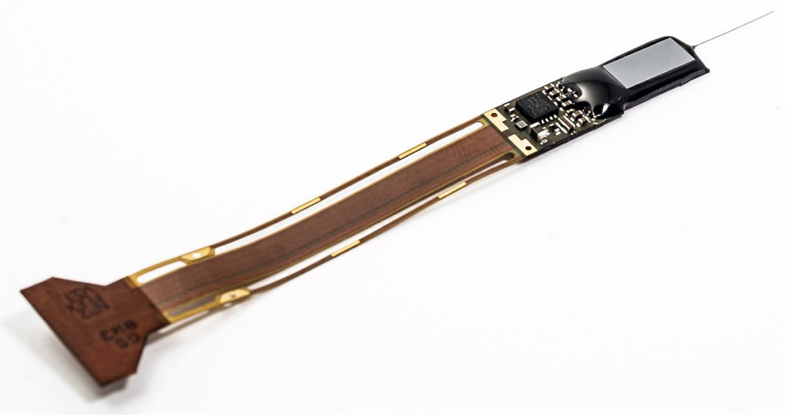
Neuropixels is an application specific integrated circuit (ASIC) with two “parts”. The shank, 70 um wide, 24 um thick, and 10 mm long contains 12 x 12 um TiN sites (recording electrodes) shown on the left drawing. The 10 mm shank has 960 sites, each with a switch to connect the site to an output line leading to the electronics in the base. Of these 960 sites, 384 can be addressed at any one time. The base has filter, a reference input multiplexer, and amplifier for each active channel. From the initial amplifier output, the signal is split into a low frequency (local field potential) and high frequency (action potential) path. Again, each active channel has a filter, and programmable amplifier for both the LFP and AP paths. The output of these 768 analog signals are fed to 32 multiplexers and 32 analog to digital converts, one A/D for each multiplexer. The digital output of the A/D’s is combined into 4 95 channel data stream and sent over the flex cable to the head stage. The probe chip is cemented to a rigid PC board with extra components. Mostly capacitors to isolate AC and DC as well as a eeprom chip that contains the probe identity. This eeprom is read by the software. The base integrated circuit must be protected from an light since light creates enormous noise for all Si electronics. The “shiny” rectangular surface visible on the left is a thin Si wafer cemented in place with opaque black epoxy.